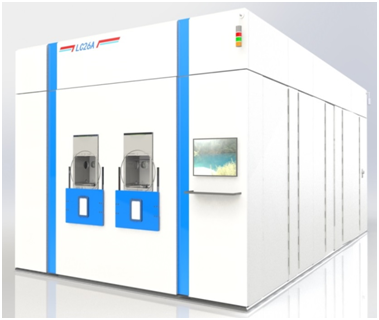
CETC Ion Implanter
  • CETC Ion Implanter

CETC Ion Implanter

We have devoted to designing and manufacturing of ion implanters since 1970s, and possesses a solid technical foundation and strong research & development capabilities. We are currently able to manufacture medium current, high current and high energy ion implanters for 8 or 12 inch wafers. Thereinto, the medium current ion implanters have been applied to mass production lines of large scale integrated circuits.


更多
  • Introduction
  • Feature
  • Parameters
  • Application scope

SiC high-temperature and high-energy ion implanter has the core technology of independent intellectual property rights, the double magnet structure of first analysis and then acceleration, the parallel beam technology, the new metal ion source, high-temperature target chamber and solid-state Al ion source, which meet the process requirements of high-energy and high-temperature state Al and N injection.

Multi plate batch chamber, single plate injection. 详情
  • 1.        The automatic high temperature target chamber system is adopted to realize the automatic transmission of vacuum film, reduce the process pollution and greatly improve the production efficiency of the equipment.;

    2.        90Degree deflection mass analyzer to achieve high-resolution ion analysis;

    3.        With hybrid scanning, horizontal electric scanning and vertical mechanical scanning, 4-inch and 6-inch wafer injection can be realized;

    4.        Long life interpenetrating thermal ion source, filament life up to more than 200 hours;

    5.        In the high temperature target heating technology, it takes only 10 minutes for the target plate to be heated from normal temperature to 500 , and the temperature difference of the whole wafer is less than 30 ;

    6.        The multi-stage constant gradient accelerating tube and voltage equalization technology are used to improve the acceleration ability and anti high pressure ignition ability. The maximum energy of ion beam reaches 400Kev (single charge);

    7.        Computer control, graphical operation interface;

    8.        Optical fiber ring communication, system anti-interference, anti fire impact.


  • 特点
  • 1.        Chip size: 6 inches (can be upgraded to 8 inches);

    2.        Energy range: 30kev ~ 400Kev (monovalent ion);

    3.        Maximum temperature of wafer: 600 ;

    4.        Injection elements: Al, B, N, p;

    5.        Injection dose: (2e11 ~ 1e16) ions / cm2;

    6.        Injection non-uniformity: < 1%;

    7.        Injection repeatability: < 1%;

    8.        Chip loading mode: automatic;

  • 参数
  • Doping injection in the manufacturing process of high voltage power electronics and high power devices based on SiC and microwave power devices based on GaAs.
  • 范围
ADVISORY MESSAGEA
  • Refresh